
Prototyping is the phase of hardware development where ideas become testable physical objects. Done well, it surfaces problems when they’re cheap and fast to fix — on a breadboard or early PCB rather than after 10,000 units have shipped. Done poorly, it creates false confidence and hides problems until they become expensive production issues. This guide walks through the complete IoT prototyping journey, from the earliest breadboard exploration through the engineering and design validation phases that precede production, with practical guidance on what to test at each stage and how to know when you’re ready to move forward.
Why Prototyping Stages Exist
A natural question: why not just design the final PCB directly and skip the intermediate stages? The answer is risk management and economics.
Cost of change escalates dramatically through the development process:
- Changing a component on a breadboard: $0, 5 minutes
- Changing a schematic before PCB is ordered: $0, 1–2 hours
- Respinning a PCB after EVT: $500–5,000 for new boards, 2–3 weeks
- Field change after product ships: $10–$100+ per device for recall, repair, or firmware workaround — plus reputational cost
Unknown unknowns multiply over time. At the concept stage, you don’t know what you don’t know. Breadboard prototyping is cheap exploration of the unknown. Each successful prototype stage reduces the uncertainty before you commit more resources.
The formal prototyping stages used in professional hardware development — EVT, DVT, PVT — encode decades of hard-won industry knowledge about what to validate and when.
Stage 1: Concept Exploration (Breadboard / Dev Board)
The first prototype is not about building a product — it’s about validating assumptions.
What you’re trying to learn:
- Does the chosen sensor actually measure what you need, with adequate accuracy?
- Does the wireless connectivity work in your intended environment?
- Can the MCU run your planned firmware with available memory?
- Does the power consumption meet your battery life targets?
- Are there any fundamental technical barriers to the intended design?
Tools for this stage:
- Breadboards for very simple, low-frequency circuits
- Development boards (Arduino, ESP32-DevKit, Nordic DK) for rapid firmware validation
- Sensor breakout boards from SparkFun, Adafruit, or similar — these provide easy connections to sensors without soldering
- Logic analyzer (Saleae Logic is the standard tool) for debugging I2C, SPI, and UART communication
- Power monitor (Nordic PPK2, or a $10 USB power monitor for rough measurements) for early power consumption estimates
Deliverables from this stage:
- Working firmware that demonstrates the core functionality
- Measured power consumption data in each operating state
- Confirmed sensor performance meets specifications
- Known firmware memory footprint
- A list of technical risks to address in subsequent stages
Common mistakes at this stage:
- Assuming the development board’s power behavior will match your final product (dev boards have LEDs, regulators, USB bridges that consume power your product won’t have — and won’t have the power optimizations your product will)
- Not measuring power consumption at this stage — “we’ll fix it later” on power often requires hardware redesign
Stage 2: Prototype PCB Design
With concept validated, design the first custom PCB. This isn’t the final product — it’s a more realistic hardware platform for firmware development and early hardware validation.
Schematic design guidelines:
Follow reference designs: MCU vendor application notes and reference schematics are valuable. They include important details that aren’t obvious from the datasheet: the specific capacitor values needed on the crystal, the antenna RF matching network, the optimal power supply filter topology. Use them as starting points, not just references.
Design for testability from day one:
- Include a JTAG/SWD debug header (even a 0.05” pitch unpopulated footprint)
- Add UART TX/RX test points
- Place test points on critical power rails and signals
- Provide a way to measure sleep current (series resistor footprint in the battery path is useful)
Power supply design:
- Size decoupling capacitors per MCU datasheet requirements — this is not optional
- Place bulk capacitors (10–100µF) and high-frequency bypass capacitors (100nF) near each power pin
- Consider EMI filtering on power inputs if running in noisy environments
Circuit protection:
- ESD protection diodes on any connector pins that could be touched or plugged/unplugged
- Current limiting and reverse polarity protection on battery input
- Thermal protection fuses if charging circuitry is included
PCB layout priorities for wireless devices:
Antenna keepout zones: The single most important layout rule for wireless IoT. Every RF module datasheet specifies a keepout area — a zone around the antenna where no copper (not even ground plane) should be present on any layer. Violating this detuning the antenna and can cause 3–10 dB of performance degradation, severely limiting wireless range.
RF trace impedance control: The transmission line from the SoC RF output to the antenna must be a controlled impedance trace (typically 50Ω). For a 2-layer PCB using 1.6mm FR4, a 50Ω microstrip is approximately 2.8mm wide. Use the PCB fab’s specific material parameters to calculate the correct width.
Ground plane integrity: Place a solid copper pour ground plane on the layer directly beneath the RF circuit. Avoid slotting the ground plane with unrelated traces, as slots act as antennas for interference.
For detailed PCB design guidance for wireless IoT devices, see our article on IoT PCB design tips.
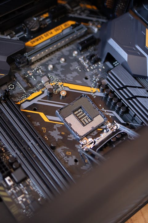
Stage 3: EVT (Engineering Validation Test)
EVT (Engineering Validation Test) — also called “Alpha prototype” or “P1” in some organizations — is the first functional prototype of your custom design. The goal is to prove that the hardware concept works.
EVT bring-up procedure:
-
Visual inspection: Before powering on, inspect the assembled board under magnification. Check for solder bridges, missing components, misoriented polarized components (capacitors, diodes, ICs with a pin 1 marker).
-
Power-on sequence: Apply power with current limiting and measure current draw on each rail before connecting the MCU. Short circuits are common on first builds.
-
Firmware bring-up: Flash minimal firmware via SWD. Verify the MCU boots (debug UART output confirms this). If using a BLE SoftDevice, flash it and verify it initializes.
-
Peripheral validation: Methodically test each peripheral:
- I2C: scan the bus and verify expected devices respond at correct addresses
- SPI: verify MOSI/MISO/CLK/CS signals with a logic analyzer during a test transaction
- UART: loopback test (connect TX to RX temporarily) to verify the UART is configured correctly
- ADC: verify readings with known reference voltages
- GPIO: toggle each output pin and verify voltage with a multimeter; trigger each input and verify the MCU reads it correctly
-
Radio validation: Send a test transmission and verify you can receive it (another radio or a spectrum analyzer); measure RSSI across a range of distances; verify antenna performance.
-
Power measurement: Measure current in each operating mode (active, idle, sleep) and compare to design targets.
EVT issue documentation: Create a formal issue list from EVT. Categorize each issue by severity and proposed resolution. This feeds into the DVT revision plan.
Typical EVT issues found:
- Power supply noise (fix: improved filtering, layout adjustment)
- ADC readings noisier than expected (fix: better analog layout, filtering)
- RF performance 3dB below expected (fix: antenna keepout violation or matching network adjustment)
- One I2C device not responding (fix: incorrect I2C address pulled down — pull-up values, address select pin)
- Higher sleep current than targeted (fix: debug which peripheral isn’t powering down properly)
Stage 4: DVT (Design Validation Test)
DVT (Design Validation Test) — also called “Beta prototype” or “P2” — incorporates EVT fixes and adds production-readiness features. The goal is to validate the design against all product requirements.
DVT design changes from EVT:
- All EVT hardware issues resolved
- Production enclosure/mechanical design integrated (if applicable)
- Manufacturing test features added (test points, programming pads, factory test mode)
- Any BOM changes (component substitutions, second sources, cost reductions)
DVT validation activities:
Functional validation: Verify all EVT issues are resolved. Run full end-to-end system tests with production firmware.
Environmental testing:
- Thermal cycling: JEDEC JESD22-A104 is a standard thermal cycling protocol. Cycling from the product’s minimum to maximum operating temperature multiple times while monitoring for intermittent failures catches solder joint reliability and thermal expansion issues.
- Humidity exposure: If the product will be deployed in humid environments (outdoors, kitchens, bathrooms), test at elevated humidity. Conformal coating may be required.
- Vibration/shock: For wearables or industrial products, test per relevant standards (MIL-STD-810, IEC 60068 series).
Regulatory pre-compliance testing: Before formal FCC/CE testing:
- Radiated emissions pre-scan to identify any frequencies where emissions exceed limits
- ESD immunity testing (IEC 61000-4-2)
- Conducted immunity testing Pre-compliance testing typically costs $2,000–$5,000 and identifies issues before the formal certification test ($5,000–$30,000 and takes 4–8 weeks).
Battery life testing: Run full-duration battery life tests. A 1-year battery life target requires either running an accelerated test (higher sample rate to reach depletion faster) or extrapolating from measured average current with a Coulomb counter.
Software validation: Run the complete test suite on DVT hardware, including edge cases and error injection tests.
Stage 5: PVT (Production Validation Test)
PVT (Production Validation Test) is the final pre-production stage. Boards are built on the actual production line with production tooling, and the manufacturing process is validated.
PVT activities:
Production build: Order a pilot production run (typically 50–500 units) from the contract manufacturer using production-representative stencils, pick-and-place, reflow, and test fixtures.
Manufacturing yield measurement: What percentage of boards pass first-pass testing? Acceptable yields vary by board complexity but 95%+ is typical for well-designed boards. Low yields indicate design or process issues.
Production test validation: Verify the production test fixture and procedure correctly identifies all known failure modes.
Firmware programming workflow validation: Verify the production firmware flashing process (including any security credential provisioning) is reliable and efficient.
Certification completion: If formal FCC/CE testing hasn’t been completed on DVT, complete it on PVT units.
Golden samples: Build and retain a set of “golden sample” units with known-good behavior to use as comparison references during production and field troubleshooting.
The Make vs. Buy Decision in Prototyping
At various stages, you face decisions about building custom hardware vs. using commercial off-the-shelf components:
Wireless modules vs. custom RF design: As discussed in choosing hardware for IoT, pre-certified wireless modules are almost always the right choice for products under ~100,000 units/year.
Custom PCBA vs. reference evaluation kits: For early proof-of-concept, buy evaluation kits and modify them rather than designing from scratch. Design from scratch begins when you have specific form factor, power, or cost requirements that off-the-shelf can’t meet.
Internal prototyping vs. outsourcing: Small teams often benefit from outsourcing PCB assembly (PCBA) even for prototypes — hand-assembling fine-pitch SMD components invites cold solder joints and damaged components that create phantom bugs.
UABit offers end-to-end prototyping support through our IoT consulting and prototyping services, from initial hardware architecture through DVT and production readiness.
Conclusion
IoT prototyping is a staged de-risking process. Each stage — concept exploration, first PCB, EVT, DVT, PVT — is designed to surface and resolve the issues most likely to appear at that level of design maturity, before they propagate to more expensive stages. The time and money invested in thorough prototyping is always returned manifold by avoided production issues, warranty claims, and recalls.
Start with exploration, validate ruthlessly at each stage, document everything, and don’t rush from one stage to the next until the open issues from the current stage are understood and addressed.
Further reading:
- JEDEC reliability standards — thermal cycling and environmental test standards
- Saleae Logic Analyzer — essential prototyping tool for protocol debugging
- KiCad PCB design software — free, open-source PCB design tool
- OSH Park prototype PCB service — US-based quality prototype PCB fabrication
- Microchip AVR and PIC prototyping tips — vendor hardware design guidance
- Electronicdesign.com PCB design resources — practical PCB design articles
IoT & AIoT Weekly
Get the best IoT development content delivered weekly. No noise, just signal.